


Press play to start listening

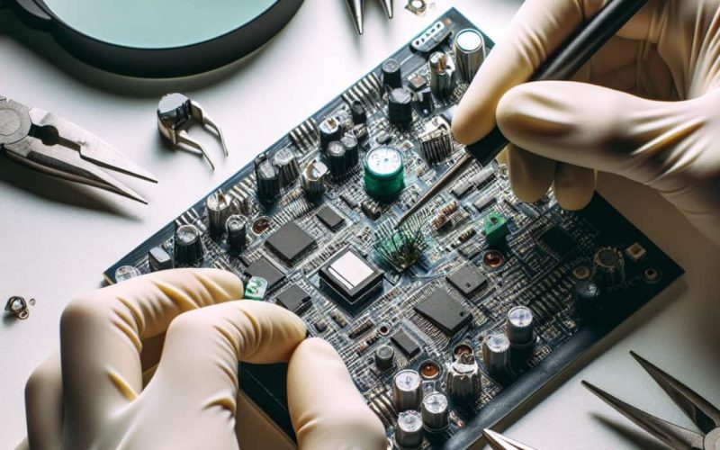
Prototype PCB assembly is the creation of an initial version of a printed circuit board design for testing and verification in electronics product development, which assesses functionality, signal integrity, and manufacturability.
In other words, prototype PCB assembly is one of the most crucial steps in electronics product development. Creating a prototype PCB brings circuit schematics to life, marking the initial physical manifestation of the design. Prototype PCB assembly encompasses this entire process.
PCB prototype assembly is the vital process of transforming electronic designs into physical boards with soldered components.
This crucial step bridges the gap between theoretical schematics and mass production, further allowing early insights and optimisations. It involves both PCB fabrication, creating physical boards from CAD designs, and assembly, soldering components based on bill of materials (BOM) requirements.
Prototyping helps mitigate risks and uncertainties in technology and manufacturing, providing a cost-effective way to validate functionality, safety, and performance before large-scale production. A good prototype assembly partner is key to the overall success of a product.
Advantages of Prototyping PCB Assembly
Exploring PCB prototypes and assemblies offers various advantages over directly engaging in mass production that are described below:
- Validation of design
- Assurance of quality
- Compatibility of components
- Economical solutions
- Time-efficient processes
Validation of Design
- Verifies and refines the design before mass production
- Identifies errors and offers an opportunity for optimization
- Reflects the final product’s functionality
Assurance of Quality
- Tests and ensures board quality and reliability
- Confirms compliance with specifications and standards
- Ensures reliable performance under different conditions
Component Compatibility
- Tests electronic components’ compatibility on the board
- Ensures efficient and effective collaboration of components
- Minimizes the risk of failure during operation
Economical Solutions
- Saves costs by identifying design errors early in the process
- Allows necessary corrections before full-scale manufacturing
- Minimizes the risk of costly mistakes
Time-Efficient Processes
- Reduces time required for testing, validation, and production
- Accelerates time-to-market for the final product
Prototype PCB Assembly: Why Do We Use It?
Verify Design Functionality
- Examine real-world performance
- Testable boards validate the design and detect flaws
- Mitigates risks before large-scale production
Accelerate Product Development
- Early verification and issue discovery
- Optimizes designs, saving over 60% in engineering time
- Significantly reduces time-to-market
Facilitate Demonstration And Funding
- Showcases viability and technology capacity
- Builds a business case for hardware startups
- Attracts early adopters and investor funding
Refine Designs For Manufacturability
- Reflects real-world manufacturing processes
- Identifies design for manufacturability (DFM) issues
- Ensures a smooth transition to mass production
Varieties of Prototype PCB Assembly
Various assembly methods and categories are employed to attach electronic components to PCB prototypes, addressing diverse production requirements, some of which are categorised below.
- Manual Assembly vs Automated SMT Assembly
- Through-Hole vs SMT Assembly
- Single-sided vs Double-sided Assembly
- Hybrid Assembly Techniques
Manual Assembly vs Automated SMT Assembly
Manual Assembly
- Manual soldering by technicians
- Suitable for low-volume orders
- Simplest method
Automated Assembly
- Automated surface mount technology assembly
- Ideal for complex board productions
- Higher efficiency
- Consistency
- Manufacturability
Through-Hole vs SMT Assembly
Through-Hole Assembly (THA):
- Connector pins pass through holes
- Respective applications
- Mixed THA parts on primarily SMT boards
- Absence of advanced features
- THA has a complex structure
Surface-Mount Technology (SMT):
- Components soldered directly onto surface pads
- Respective applications
- Advanced technology allows combining both
- SMT also has respective applications
Single-sided vs Double-sided Assembly
Single-Sided Assembly:
- Components are placed and soldered on one side
- Suitable for less complex designs
Double-Sided Assembly:
- Parts soldered on both sides, allowing higher component density
- Ideal for more intricate and densely populated PCBs
Hybrid Assembly Techniques
Advanced Manufacturing Capabilities:
- Utilizes state-of-the-art manufacturing capabilities
- Optimizes production flexibility
Component Mixtures on Boards:
- Combines 0201 size tiny chips with larger SMT parts and some through-hole passives
- Allows hybrid assembly on double-sided boards
How To Assemble A Prototype PCB
Building prototype PCBs involves following standard assembly stages to turn CAD designs into functioning boards. This can be done through automated SMT lines or manual assembly processes.
Prototype PCB Assembly Process Steps:
- SMT Pick-and-Place Stage
- SMT Reflow Soldering
- Cleaning/Washing
- AOI and Functional Testing
- Final Programming/Flashing
SMT Pick-and-Place Stage
- Utilizes advanced pick-and-place machines for a precise component population
- Based on optimised programming and feeder setup
- Ensures high precision and traceability
SMT Reflow Soldering
- Boards pass through industrial reflow ovens after accurate component positioning.
- Enables simultaneous precision soldering of SMT parts
- Carefully optimised thermal profiling for permanent attachment
Cleaning/Washing
- After rework, cleaning solutions wash flux residues off board surfaces
- Ensures thorough removal for ionic cleanliness
AOI and Functional Testing
- Automated optical inspection checks component placement
- Rigorous functional testing examines board performance metrics
- Ensures specification compliance using fixture testing
Final Programming/Flashing
- Downloads optimised software/firmware builds to boards
- Completes prototype PCB assembly for design validation
- Precedes shipping to customers
Final Thoughts
Prototype PCB assembly is vital for electronics product development, verifying designs and validating concepts. Quality builds impact design optimizations and securing financing. Balancing costs, responsive turnarounds, and technical alignment are crucial. Bittele offers professional turnkey services, reshaping ideas into testable boards for commercial success. With a focus on exceptional quality and responsive support, choosing the right assembly partner is key for impactful innovation trajectories.
People Also Asked
Q: How do I make a PCB prototype?
A: The PCB prototype assembly involves the following steps:
- Design
- Schematic creation
- BOM generation
- Routing design
- Thorough checks
Fabrication includes:
- Creating photo films
- Printing layers
- Fusing
- Drilling
- Plating
- Applying finishes
The assembly stage includes:
- Stencilling
- Pick and place
- Reflow soldering
- Inspection
- Inserting through-hole components
- Conducting functionality tests
Q: What is a PCB prototyping machine?
A: An eco-friendly PCB machine is utilized throughout the entire PCB production process, ensuring environmentally conscious practices from design validation to board assembly.